In modern product development, the boundaries between electronics and mechanical design are rapidly disappearing. A printed circuit board (PCB) no longer exists in isolation—it must coexist perfectly with its enclosure, connectors, and thermal environment.
Many engineers have experienced the frustration of misaligned holes, warped casings, or PCBs that fail to fit after final assembly. These issues often trace back to one root cause: the lack of early coordination between PCB assembly and plastic enclosure manufacturing.
Leading electronic manufacturing service (EMS) providers have demonstrated that a tightly controlled PCB assembly process not only ensures electrical reliability but also enables smoother integration during mechanical assembly. When electrical and mechanical teams collaborate early, product consistency and time-to-market improve significantly.

Early Collaboration: Applying Design for Manufacturability (DFM) Principles
Effective collaboration begins long before production starts. In many cases, PCB design and mold design proceed independently, which inevitably leads to misalignment, rework, and increased cost. Implementing Design for Manufacturability (DFM) principles helps prevent these issues.
At the design stage, it’s critical to synchronize both sides on:
- Mounting interface alignment – ensuring screw holes, pillars, and slots align with PCB fixing points.
- Connector positioning – verifying port locations and component heights relative to shell openings.
- Thermal and clearance planning – allocating sufficient distance for heat dissipation and shielding.
CAD data exchange formats, such as STEP or DXF, should be part of every project handoff. When electronic and mold engineers share accurate 3D references, potential interference can be detected and resolved before tooling begins. This collaborative validation reduces both risk and development lead time.
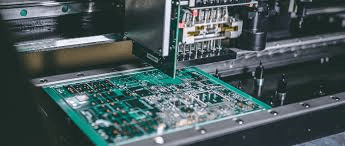
The Role of PCB Assembly in Structural Integration
PCB assembly defines the dimensional foundation of every electronic device. A deviation of just fractions of a millimeter during surface-mount (SMT) or wave soldering may cause the entire assembly to shift.
High-quality EMS providers implement stringent control processes to mitigate this. For example, Leadsintec applies automated optical inspection (AOI), X-ray testing, and functional validation to ensure uniform soldering and flatness across each board. Such consistency directly supports mechanical fit during enclosure assembly.
Beyond electrical reliability, PCB flatness, component placement accuracy, and overall dimensional stability influence screw alignment, connector engagement, and sealing integrity. In high-volume production, these parameters must remain within statistical process control limits to prevent cumulative tolerance errors.
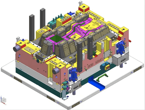
Mechanical Precision: Mold Design and Injection Molding Alignment
From the mechanical perspective, precision mold design is equally crucial. The injection-molded enclosure defines how the PCB is positioned, supported, and protected. Inaccurate mold dimensions, even by 0.1 mm, can cause mounting misalignment or undue stress on solder joints.
When designing enclosures, engineers should account for:
- Material shrinkage – ABS, PC, and PA have distinct shrink rates that affect hole spacing and wall thickness.
- Tolerance stack-up – cumulative deviations from multiple parts that influence fit accuracy.
- Stress distribution – snap-fit or latch structures must not impose bending forces on the PCB.
Material selection also impacts reliability. For example, PC provides higher dimensional stability but transmits heat faster to nearby components, while ABS is easier to process but less stable under prolonged thermal load. A balanced approach between mechanical performance and electronic safety is essential.
Cleanroom molding environments and dimensional inspection systems further ensure consistent quality for high-precision assemblies.
Common Integration Challenges and Practical Solutions
Despite best efforts, integration between electronics and enclosure often presents recurring challenges. Below are five common issues and corresponding preventive strategies:
| Challenge | Cause | Recommended Solution |
| Hole misalignment | Independent tolerance control between PCB and mold | Conduct a combined 3D tolerance analysis and validation before tooling |
| Heat accumulation | Inadequate thermal design or material selection | Incorporate venting channels, heat spreaders, or conductive inserts |
| EMI susceptibility | Plastic enclosure without proper grounding or shielding | Add conductive coatings, grounding clips, or internal metallic layers |
| Assembly-induced stress | Over-constrained fixing points or screw torque | Use flexible spacers and controlled torque tightening |
| Limited maintainability | Fully enclosed structures or glued joints | Adopt modular fastening or removable panels for service access |
Addressing these aspects early ensures stable integration and long-term reliability of both electrical and mechanical subsystems.
Coordinating PCB and Enclosure Suppliers: A Collaborative Approach
Cross-supplier collaboration is the foundation of successful integration. Too often, PCB assembly vendors and mold makers operate separately, leading to mismatched expectations and design revisions.
A robust workflow typically includes:
- Preliminary DfM review involving both EMS and tooling teams.
- 3D assembly validation using digital mockups.
- Trial production (T0/T1) to confirm structural and functional fit.
- Functional and environmental testing before mass production.
By partnering with experienced PCB assembly manufacturers such as Leadsintec, you ensure the electronic subsystem is validated and dimensionally stable before mold fabrication begins. This integrated process minimizes rework, accelerates validation cycles, and supports higher first-pass yield.
At Kemal, we have observed that projects adopting parallel collaboration achieve faster development timelines, lower scrap rates, and better final assembly performance compared with traditional sequential workflows.
Future Trends: Smart Manufacturing and Digital Prototyping
The future of integrated product design lies in digitalization. Advanced manufacturing technologies such as digital twins, rapid prototyping, and data-driven process control now allow simultaneous validation of electronic and mechanical systems.
Digital twins create a real-time virtual model of the product, predicting thermal behavior, stress distribution, and assembly tolerances before physical production. Meanwhile, rapid prototyping—via 3D-printed enclosures and functional PCB samples—enables early fit testing and user validation.
Smart manufacturing platforms also link PCB assembly data with mold production metrics, allowing engineers to trace every dimension and parameter. The result is a more agile, transparent, and reliable production environment.
Conclusion: Achieving Precision Through Integration
The integration of PCB assembly and plastic enclosure manufacturing is no longer optional—it is a prerequisite for modern, high-reliability products. Aligning electrical performance with mechanical precision demands early collaboration, disciplined process control, and a shared understanding of manufacturing constraints.
By uniting precision mold makers with professional PCB assembly partners like Leadsintec, you can establish a production ecosystem where every design detail contributes to long-term performance and user satisfaction.
As product complexity continues to rise, the most successful manufacturers will be those who treat integration not as a challenge, but as a competitive advantage built into every stage of their design and production process.
